SupraSol WLT-M, process for the Micro-Bump Pure Tin plating of High Bandwidth Memory (HBM) semiconductor, has been qualified by SK Hynix with support from the “Next-generation intelligent semiconductor development project”, in collaboration with Raon International, Korea Electronics Technology Institute and Sungkyunkwan University have successfully fulfilled SK Hynix’s quality criteria for Pure Tin Micro-Bump plating materials, performance and reliability.
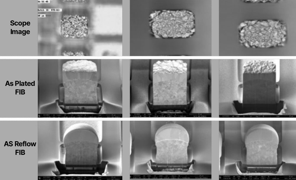
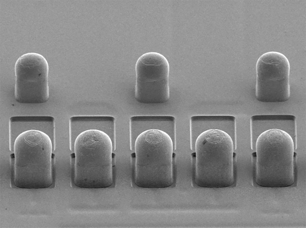
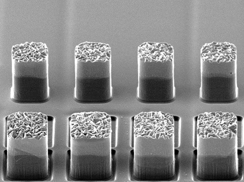
SupraSol WLT-M is designed to meet the requirements of next-generation semiconductor plating processes, such as those used in SK Hynix’s HBM semiconductor. It is applicable to the Micro-Bump Pure Tin plating process, particularly in the capping process on Cu Pillars. It enables high-speed plating with high current density and has demonstrated its excellence by securing a Within-Wafer (WIW) uniformity of 2.98% on mass production-grade 12-inch wafers, even in complex and diverse fine patterns.
We kindly ask for your continued interest and support.
Thank you.


